US12282180 - Stealth device
The patent describes a stealth device designed to absorb and selectively transmit near-infrared light using a complex arrangement of conductive thin-film patterns and dielectric layers. This technology aims to enhance stealth capabilities against various electromagnetic wavelengths, potentially applicable in military or surveillance contexts.
Claim 1
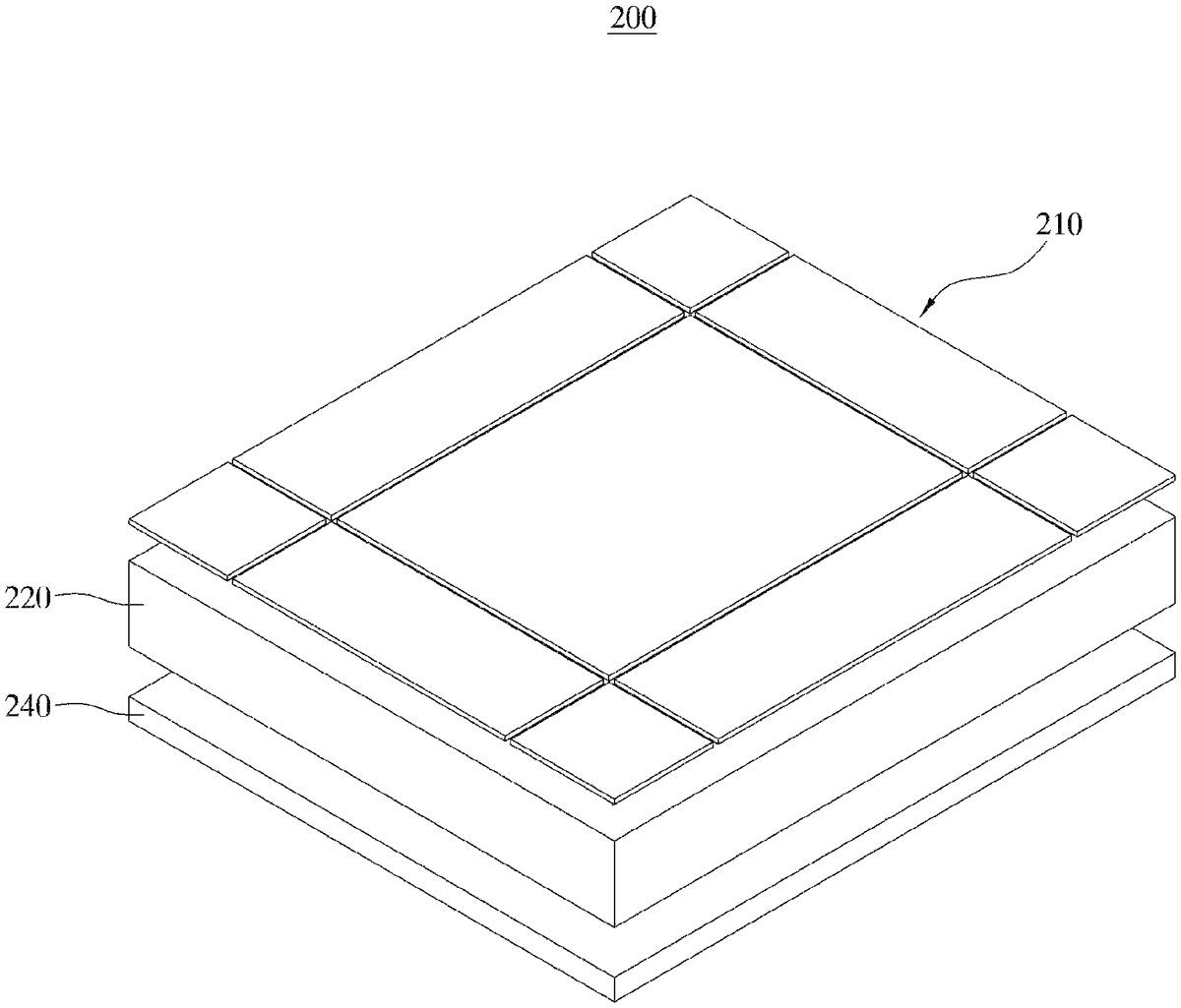
- A stealth device comprising: a wavelength-selective absorption pattern layer including at least one conductive thin-film pattern having near-infrared light transmissive holes defined therein capable of selectively transmitting near-infrared light therethrough; a near-infrared absorption layer disposed below the wavelength-selective absorption pattern layer to absorb near-infrared light which has passed through the near- infrared light transmissive holes; and a dielectric layer disposed between the wavelength-selective absorption pattern layer and the near-infrared absorption layer and made of a dielectric material, wherein the wavelength-selective absorption pattern layer is composed of a plurality of unit areas, wherein each unit area has a square shape having two sides parallel to a first direction and two sides parallel to a second direction perpendicular to the first direction, wherein in each unit area, the conductive thin-film pattern includes: a first thin-film pattern having a planar shape of a first square having two sides parallel to the first direction and two sides parallel to the second direction, wherein each side of the first square has a first length; a second thin-film pattern having a planar shape of a second square having two sides parallel to the first direction and two sides parallel to the second direction, wherein each side of the second square has a second length smaller than the first length, wherein a diagonal line of the first thin-film pattern and a diagonal line of the second thin-film pattern coincide with one of two diagonal lines of the unit area; and two third thin-film patterns, wherein each of the two third thin-film patterns has a rectangular planar shape in which a long side parallel to the second direction has the first length and a short side parallel to the first direction has the second length, wherein one of the two third thin-film patterns is disposed adjacent to a first side of the first thin-film pattern, while the other thereof is disposed adjacent to a second side of the first thin-film pattern perpendicular to the first side of the first thin-film pattern. a wavelength-selective absorption pattern layer including at least one conductive thin-film pattern having near-infrared light transmissive holes defined therein capable of selectively transmitting near-infrared light therethrough; a near-infrared absorption layer disposed below the wavelength-selective absorption pattern layer to absorb near-infrared light which has passed through the near- infrared light transmissive holes; and a dielectric layer disposed between the wavelength-selective absorption pattern layer and the near-infrared absorption layer and made of a dielectric material, wherein the wavelength-selective absorption pattern layer is composed of a plurality of unit areas, wherein each unit area has a square shape having two sides parallel to a first direction and two sides parallel to a second direction perpendicular to the first direction, wherein in each unit area, the conductive thin-film pattern includes: a first thin-film pattern having a planar shape of a first square having two sides parallel to the first direction and two sides parallel to the second direction, wherein each side of the first square has a first length; a second thin-film pattern having a planar shape of a second square having two sides parallel to the first direction and two sides parallel to the second direction, wherein each side of the second square has a second length smaller than the first length, wherein a diagonal line of the first thin-film pattern and a diagonal line of the second thin-film pattern coincide with one of two diagonal lines of the unit area; and two third thin-film patterns, wherein each of the two third thin-film patterns has a rectangular planar shape in which a long side parallel to the second direction has the first length and a short side parallel to the first direction has the second length, wherein one of the two third thin-film patterns is disposed adjacent to a first side of the first thin-film pattern, while the other thereof is disposed adjacent to a second side of the first thin-film pattern perpendicular to the first side of the first thin-film pattern. a first thin-film pattern having a planar shape of a first square having two sides parallel to the first direction and two sides parallel to the second direction, wherein each side of the first square has a first length; a second thin-film pattern having a planar shape of a second square having two sides parallel to the first direction and two sides parallel to the second direction, wherein each side of the second square has a second length smaller than the first length, wherein a diagonal line of the first thin-film pattern and a diagonal line of the second thin-film pattern coincide with one of two diagonal lines of the unit area; and two third thin-film patterns, wherein each of the two third thin-film patterns has a rectangular planar shape in which a long side parallel to the second direction has the first length and a short side parallel to the first direction has the second length, wherein one of the two third thin-film patterns is disposed adjacent to a first side of the first thin-film pattern, while the other thereof is disposed adjacent to a second side of the first thin-film pattern perpendicular to the first side of the first thin-film pattern.
Google Patents
https://patents.google.com/patent/US12282180
USPTO PDF
https://image-ppubs.uspto.gov/dirsearch-public/print/downloadPdf/12282180